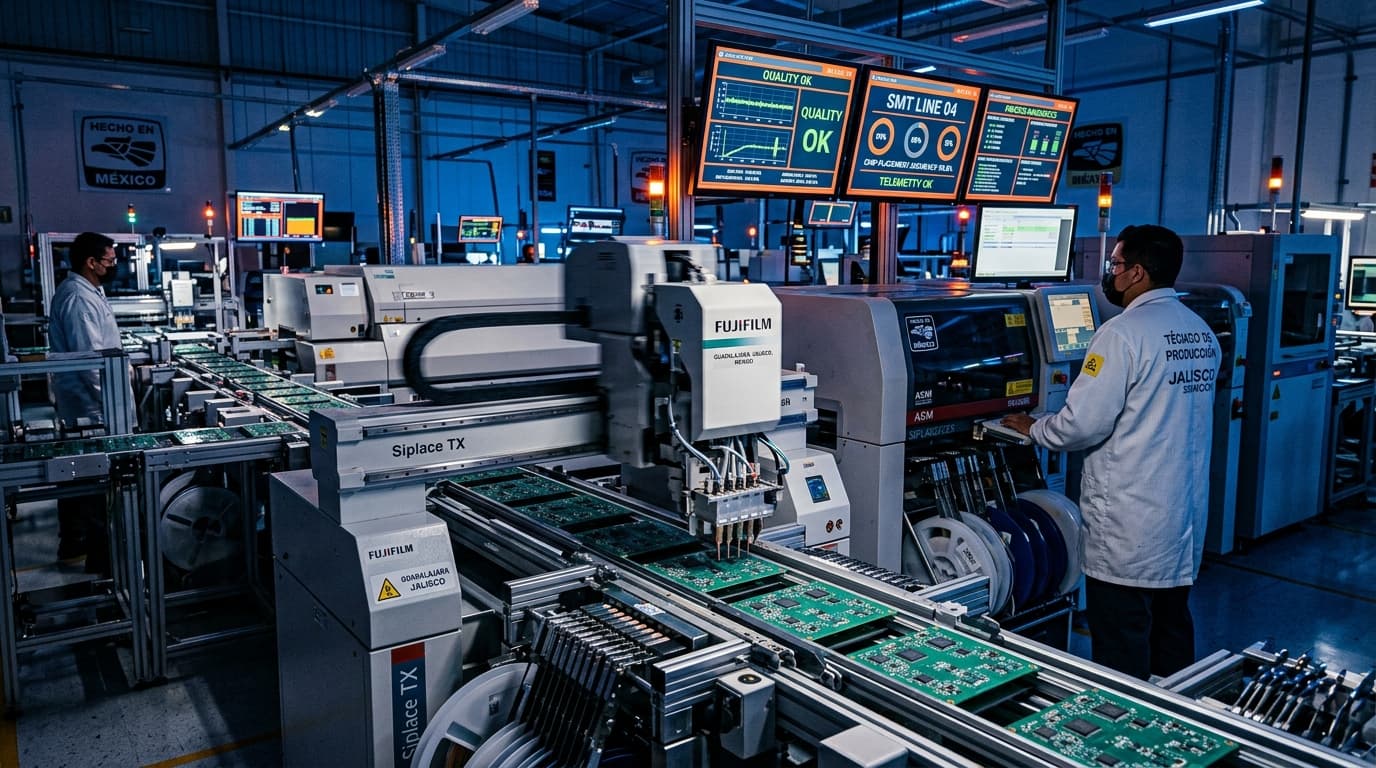
Semiconductor & Advanced Electronics Nearshoring: Navigating Mexico's CHIPS Act Integration, Guadalajara Clusters & ITAR Compliance
Master semiconductor & electronics nearshoring to Mexico. Technical guide on U.S. CHIPS Act OSAT integration, Guadalajara vs. Baja clusters, ITAR/EAR compliance & USMCA RVC.
Semiconductor & Advanced Electronics Nearshoring: Navigating Mexico's CHIPS Act Integration, Guadalajara Clusters & ITAR Compliance
An Executive Engineering & Trade Compliance Blueprint on North American Microelectronics Nearshoring, Tier 1 EMS Ecosystems, Defense Export Controls, Cleanroom Utilities, and USMCA Chapter 4 Rules of Origin
By Denisse Martinez, Senior Technical SEO & Trade Compliance Specialist Published September 15, 2026 | Nearshore Navigator Executive Advisory
Executive Summary: The Geopolitics of Advanced Electronics in Mexico
Mexico has emerged as North America's premier advanced electronics manufacturing hub, driven by U.S. CHIPS Act supply chain integration, Section 301 China tariffs, and USMCA origin requirements. By offering mature Tier 1 EMS clusters, cross-border logistics lanes, and cost-effective engineering talent, Mexico enables OEMs to de-risk critical microelectronics while maintaining tariff-free access to U.S. markets.
The global semiconductor and advanced electronics manufacturing paradigm has shifted permanently from a low-cost, transpacific optimization model to an insulated, regional resilience framework. Driven by intensifying geopolitical friction between Washington and Beijing, escalating Section 301 tariff enforcement, and statutory mandates under the National Defense Authorization Act (NDAA Sections 889 and 5949) prohibiting federal procurement of Chinese logic and memory semiconductors, North American original equipment manufacturers (OEMs) are aggressively reshoring and nearshoring their electronics production lifecycles.
+-----------------------------------------------------------------------------------------+
|                  TRANS-PACIFIC VS. NORTH AMERICAN ELECTRONICS VALUE CHAIN               |
+-----------------------------------------------------------------------------------------+
| METRIC                       | ASIAN OFFSHORE MODEL       | MEXICO NEARSHORE CORRIDOR   |
+------------------------------+----------------------------+-----------------------------+
| Transit Lead Time (Fab to ATP)| 28 - 45 Days (Maritime)    | 24 - 48 Hours (Bonded Land) |
| Tariff Exposure (Section 301)| Up to 25% - 50% Ad Valorem | 0% Duty under USMCA Ch. 4   |
| Defense Regulatory Pathway   | Prohibited for ITAR/DoD    | Permitted via DDTC TAA/MLA  |
| Working Capital Cash Cycle   | 90 - 120 Days Inventory    | 21 - 35 Days Inventory      |
| Critical IP / Data Flight    | Severe Jurisdiction Risk   | CMMC / USMCA Chapter 20 IP  |
+-----------------------------------------------------------------------------------------+
Historically, OEMs decoupled semiconductor design and fabrication from the downstream processes of Assembly, Testing, and Packaging (ATP), outsourcing the labor-intensive packaging phase to Southeast Asian hubs in Taiwan, Malaysia, Vietnam, and mainland China. However, recent disruptions—spanning shipping container rate volatility, naval chokepoints in the Taiwan Strait, and aggressive U.S. Department of Commerce Bureau of Industry and Security (BIS) export controls—have rendered this dispersed supply chain untenable for mission-critical industrial, automotive, and defense hardware.
Mexico has captured the lion's share of this strategic realignment. Bolstered by its $80+ billion annual electronics manufacturing export footprint, mature industrial clusters across Jalisco, Baja California, Chihuahua, and Nuevo León, and an established workforce of more than 400,000 electronics assembly operators and technicians, Mexico is the operational linchpin of the North American semiconductor corridor. To evaluate detailed financial and operational modeling across various Mexican states, executives can utilize our Nearshore Landed Cost Calculator to stress-test direct labor, utility, and freight differentials.
The U.S. CHIPS Act & Mexico's Role in Semiconductor ATP / Packaging
Under Section 103 of the U.S. CHIPS Act and the State Department's ITSI Fund, Mexico is officially integrated as North America's back-end semiconductor corridor. While U.S. mega-fabs in Arizona and Texas handle front-end wafer fabrication, Mexico provides high-volume, cost-competitive Assembly, Testing, and Packaging (ATP/OSAT) services, dramatically reducing transpacific supply chain bottlenecks and geopolitical exposure.
When the United States enacted the Creating Helpful Incentives to Produce Semiconductors (CHIPS) and Science Act of 2022 (Public Law 117-167), federal policymakers recognized an inescapable structural reality: subsidizing over $52 billion in domestic front-end wafer fabrication (wafer fabs) in Arizona (TSMC, Intel), Texas (Samsung, Texas Instruments), Ohio (Intel), and New York (Micron) would fail to secure the supply chain if finished silicon wafers still had to cross the Pacific Ocean to be diced, encapsulated, wire-bonded, and tested.
To prevent this fatal vulnerability, Section 103 of the CHIPS Act established the International Technology Security and Innovation (ITSI) Fund, allocating $500 million ($100 million annually over five years) to the U.S. Department of State to coordinate secure international semiconductor supply chains with trusted democratic allies. In 2023 and 2024, the U.S. State Department formally partnered with the Mexican Ministry of Economy (Secretaría de Economía) to conduct comprehensive technical capability assessments and expand Mexico's capacity for back-end semiconductor operations.
NORTH AMERICAN SEMICONDUCTOR CORRIDOR

  +---------------------------------------------------------------------------------+
  |                  FRONT-END WAFER FABRICATION (CAPEX INTENSIVE)                  |
  |  • TSMC (Phoenix, AZ)      • Intel (Chandler, AZ & New Albany, OH)              |
  |  • Samsung (Taylor, TX)    • Texas Instruments (Sherman, TX)                    |
  +---------------------------------------------------------------------------------+
                                         |
                                         | [Secured Temperature-Controlled
                                         |  Air & Bonded Overland Freight]
                                         v
  +---------------------------------------------------------------------------------+
  |                MEXICO BACK-END ATP / OSAT CORRIDOR (LABOR & SMT READY)          |
  |  • Mexicali / Tijuana (Baja) : RF packaging, Wafer Dicing, Aerospace Micro-BGA  |
  |  • Guadalajara (Jalisco)     : Silicon Validation, Substrate Assembly, Auto ECUs|
  +---------------------------------------------------------------------------------+
                                         |
                                         | [24 - 48 Hour Bonded FAST Lane Transit]
                                         v
  +---------------------------------------------------------------------------------+
  |               FINAL SYSTEM INTEGRATION & OEM COMMERCIALIZATION                  |
  |  • U.S. Defense Primes (Lockheed Martin, Raytheon, Northrop Grumman)            |
  |  • North American Automotive Assembly (Detroit 3, Tesla, BMW, GM Silao)         |
  +---------------------------------------------------------------------------------+
The Technological Value Chain: Front-End Lithography vs. Back-End Packaging
Semiconductor manufacturing divides sharply into two distinct industrial disciplines:
- $0
Guadalajara vs. Mexicali vs. Tijuana: Regional Tech Ecosystem Comparison
Guadalajara leads Mexico in semiconductor design, complex software engineering, and high-volume Tier 1 contract manufacturing (EMS). Mexicali specializes in precision microelectronics, RF semiconductor packaging, and direct aerospace integration with Arizona's chip corridor. Tijuana dominates high-mix, medium-to-high-volume printed circuit assembly (PCBA), medical devices, and defense electronics with immediate same-day access to Southern California supply chains.
Selecting an operational location for advanced electronics manufacturing in Mexico requires aligning component complexity, end-market velocity, and technical infrastructure with regional capabilities. The three primary technological epicenters—Guadalajara (Jalisco), Mexicali (Baja California), and Tijuana (Baja California)—present distinct operational advantages.
1. Guadalajara, Jalisco: "The Silicon Valley of Mexico"
Guadalajara’s electronics ecosystem was forged over four decades ago when global technology pioneers, including IBM, Hewlett-Packard, and Motorola, established core manufacturing facilities along the Periférico corridor. Today, Jalisco hosts Mexico’s most sophisticated technology ecosystem, blending massive high-density Tier 1 Electronic Manufacturing Services (EMS) providers with world-class engineering and semiconductor validation centers.
- $0
2. Mexicali, Baja California: The Microelectronics & Packaging Frontier
While Guadalajara is the leader in systems engineering and Tier 1 EMS, Mexicali has distinguished itself as Mexico's specialized microelectronics and cleanroom semiconductor packaging powerhouse.
- $0
3. Tijuana, Baja California: High-Mix SMT, Defense & Medical Precision
Tijuana represents the world's most concentrated industrial border city, boasting over 600 export maquiladoras. In advanced electronics, Tijuana specializes in high-mix, medium-to-high-volume SMT manufacturing, aerospace harnesses, optical communication devices, and Class II/III medical electronics.
- $0
Regional Technical Ecosystem Comparison Matrix
The following structured matrix compares Mexico's primary electronics manufacturing clusters across eight critical operational dimensions:
| Comparative Dimension | Guadalajara (Jalisco) | Mexicali (Baja California) | Tijuana (Baja California) |
|---|---|---|---|
| Primary Specialization | Tier 1 EMS, High-Volume PCBA, IC Design & Validation | OSAT / ATP, RF Packaging, Aerospace Microelectronics | High-Mix SMT, Medical PCBA, Defense Avionics & Wire Harnesses |
| Anchor Tier 1 Employers | Flex, Jabil, Sanmina, Foxconn, Benchmark Electronics, Intel GDC | Skyworks Solutions, Collins Aerospace, Gulfstream, Honeywell | Foxconn, Benchmark Electronics, Kyocera, Poly (HP), Safran |
| Logistics Proximity to U.S. | 12-16 hrs to Laredo, TX (Overland Rail/Highway) | 3.5 hrs to Phoenix, AZ (Interstate 8 Corridor) | 30 mins to San Diego, CA (Otay Mesa Commercial Gate) |
| Cleanroom Availability | High (ISO Class 7/8 in major Tier 1 campuses) | Extreme (ISO Class 5/7 dedicated microelectronics) | High (ISO Class 7/8 medical & aerospace certified) |
| Engineering Talent Focus | IC Layout, Embedded Systems, Firmware, High-Speed RF | Microelectronics Packaging, Wafer Dicing, Cleanroom Automation | NPI Industrial Engineering, DFM, IPC-A-610 Soldering, Lean SMT |
| Power Infrastructure (CFE) | Mature industrial parks; 115 kV substations available | Dual-grid geothermal/gas stability; high MVA capacity | Dense grid; requires dedicated private substation verification |
| Average Burdened Tech Wage | $7.50 - $11.00 USD / hr (Fully Burdened Technician) | $7.80 - $11.50 USD / hr (Northern Border Minimum Applied) | $7.80 - $11.50 USD / hr (Northern Border Minimum Applied) |
| Key Export Gateway | Guadalajara Int'l Cargo Airport (GDL) & Laredo Port | Calexico East Commercial Port (Direct to I-8 / Phoenix) | Otay Mesa Commercial Port (Direct to CA-905 / San Diego) |
ITAR & EAR Dual-Use Compliance in Mexican Electronics Manufacturing
Manufacturing defense or dual-use electronics in Mexico requires strict adherence to ITAR (22 CFR Parts 120-130) and EAR (15 CFR Parts 730-774). U.S. contractors must secure approved Technical Assistance Agreements (TAAs) or export licenses before transferring technical data. Mexican facilities must implement segregated physical manufacturing cells, biometric access controls, and air-gapped, CMMC-aligned data networks to prevent unauthorized foreign national access.
As U.S. aerospace and defense prime contractors nearshore Tier 2 and Tier 3 electronic assemblies—such as radar digital signal processors, missile guidance boards, and military communications modules—compliance with federal export controls becomes an absolute legal prerequisite. Transferring electronics manufacturing to Mexico does not exempt an enterprise from U.S. export jurisdiction.
+-----------------------------------------------------------------------------------------+
|                  U.S. DEFENSE EXPORT CONTROL JURISDICTIONAL BREAKDOWN                   |
+-----------------------------------------------------------------------------------------+
| REGULATORY REGIME    | GOVERNING BODY              | CONTROL LIST & SCOPE               |
+----------------------+-----------------------------+------------------------------------+
| ITAR                 | U.S. Department of State    | United States Munitions List (USML)|
| (22 CFR Parts 120-130)| DDTC                        | Category XI (Military Electronics) |
|                      |                             | Category XII (Fire Control/Optics) |
|                      |                             | Category XV (Spacecraft Systems)   |
+----------------------+-----------------------------+------------------------------------+
| EAR                  | U.S. Department of Commerce | Commerce Control List (CCL)        |
| (15 CFR Parts 730-774)| BIS                         | ECCN 3A001 (Electronic Components) |
|                      |                             | ECCN 5A002 (Information Security)  |
|                      |                             | ECCN 9A515 (Space & Satellite)     |
+----------------------+-----------------------------+------------------------------------+
The "Deemed Export" Rule and Cross-Border Technical Data Transfers
Under 22 CFR § 120.17 of the ITAR and 15 CFR § 734.13 of the EAR, disclosing or releasing controlled technical data—including computer-aided design (CAD) files, Gerber layout layers, firmware source code, bill-of-materials schematics, or surface-mount pick-and-place optimization files—to a foreign national (including a Mexican citizen working inside a Mexican plant) is legally deemed an export to that person's home country.
Without prior statutory authorization from the U.S. Government, any such data transfer constitutes a federal violation punishable by civil penalties exceeding $1 million per violation, statutory debarment, and criminal prosecution under 22 U.S.C. § 2778.
Mandatory U.S. Licensing Instruments
To lawfully manufacture ITAR-controlled electronics in Mexico, the U.S. exporter of record and the Mexican manufacturing entity must establish formal licensing mechanisms:
- $0
Physical Security and Plant Segregation: The "Cage Within a Plant" Model
A Mexican electronics facility cannot process commercial consumer products and ITAR defense articles on the same open manufacturing floor without breaching export regulations. Mexican contract manufacturers and shelter operators satisfy DDTC standards by engineering physically segregated production environments:
- $0
Cybersecurity and CMMC / NIST SP 800-171 Network Isolation
Logical data security must match physical perimeter controls. In accordance with U.S. Department of Defense mandates under the Cybersecurity Maturity Model Certification (CMMC 2.0 Level 2) and NIST SP 800-171:
- $0
Infrastructure Imperatives: SMT Line Cleanrooms, Power Drops & ESD Standards
Deploying high-reliability surface mount technology (SMT) and microelectronics lines in Mexico requires 2 MVA+ dedicated medium-voltage substation power drops, clean power conditioning, and ANSI/ESD S20.20-certified conductive flooring. Facilities must maintain ISO Class 7 or 8 cleanrooms with positive pressure, 40–60% relative humidity, Class 1.2.1 compressed dry air, and high-purity nitrogen feeds to prevent component oxidation and defects.
Advanced microelectronics and semiconductor packaging cannot function in standard industrial warehouse space. High-density printed circuit assemblies, 01005 passive components, micro-Ball Grid Arrays (micro-BGAs) with 0.3mm ball pitch, and bare silicon wire-bonding demand specialized physical plant infrastructure.
+-----------------------------------------------------------------------------------------+
|                  HIGH-PRECISION SMT MANUFACTURING INFRASTRUCTURE MATRIX                 |
+-----------------------------------------------------------------------------------------+
| PARAMETER                 | SPECIFICATION                   | OPERATIONAL PURPOSE       |
+---------------------------+---------------------------------+---------------------------+
| Electrical Substation     | 2.0 - 5.0 MVA (13.8kV / 34.5kV) | Power multi-zone ovens,   |
| Capacity & Drops          | Medium-Voltage Dedicated Feed   | high-speed pick-and-place |
+---------------------------+---------------------------------+---------------------------+
| Power Quality / Backup    | Dynamic Voltage Restorer + UPS  | Mitigate sags (<20ms);    |
|                           | N+1 Diesel Gensets (10-sec synch)| eliminate reflow board loss|
+---------------------------+---------------------------------+---------------------------+
| Cleanroom Classification  | ISO 14644-1 Class 7 (Fed Std    | Die attach, wire bonding, |
|                           | 10,000) or Class 8 (100,000)    | flip-chip & AOI opticals  |
+---------------------------+---------------------------------+---------------------------+
| Electrostatic Discharge   | ANSI/ESD S20.20 & IEC 61340-5-1 | Conductive tile/epoxy;    |
| (ESD) Flooring            | Resistance: 1.0x10^6 - 1.0x10^9 | Prevent latent gate oxide |
|                           | ohms to ground                  | breakdown on sensitive ICs|
+---------------------------+---------------------------------+---------------------------+
| Process Atmosphere        | 99.999% High-Purity Nitrogen    | O2 levels < 50 ppm in     |
| (Reflow Ovens)            | (5.0 Grade Liquid N2 Dewar/Bulk)| reflow; perfect wetting   |
+---------------------------+---------------------------------+---------------------------+
| Compressed Dry Air (CDA)  | ISO 8573-1 Class 1.2.1          | Moisture dew point -40°C; |
|                           | Oil-free rotary screw compressor| Zero oil contamination    |
+---------------------------+---------------------------------+---------------------------+
| Humidity & Temperature    | 40% - 60% Relative Humidity (RH)| Prevent static (<40%) and |
| Control Envelope          | 21°C ± 2°C (70°F ± 3°F) Temp    | solder popcorning (>60%)  |
+-----------------------------------------------------------------------------------------+
1. Dedicated Medium-Voltage Electrical Drops (2 MVA to 5 MVA)
A standard electronics manufacturing plant operating four to eight automated SMT lines—incorporating dual-lane stencil printers, 3D solder paste inspection (SPI), multi-head high-speed pick-and-place machines (mounting 80,000 to 120,000 components per hour), 12-to-14 zone convection reflow ovens, and automated optical inspection (AOI) units—consumes massive electrical loads.
Substation Sizing: SMT lines and their supporting cleanroom chillers require a dedicated medium-voltage (13.8 kV or 34.5 kV) electrical substation delivering between 2.0 MVA and 5.0 MVA from the Comisión Federal de Electricidad (CFE). OEMs must verify whether an industrial park has readily available kVA capacity or if a formal CFE interconnection study (estudio de factibilidad*) and transformer installation will require a 6-to-12 month lead time.
- $0
2. Cleanroom Architecture: ISO 14644-1 Standards
While consumer electronic box assembly can occur in conditioned ambient factory air, semiconductor ATP, wafer dicing, die attach, wire bonding, and high-density flip-chip assembly require certified cleanrooms:
- $0
3. Electrostatic Discharge (ESD) Mitigation (ANSI/ESD S20.20)
Modern sub-micron silicon chips feature gate oxide layers only a few nanometers thick. An electrostatic discharge of merely 50 volts—imperceptible to human touch—can rupture gate dielectrics, causing catastrophic component failure or insidious latent defects that manifest months later in field operation.
- $0
5-Step Electronics Nearshoring Deployment & Supplier Qualification Protocol
Successfully onboarding an advanced electronics manufacturing operation in Mexico follows a structured 5-step technical protocol: executing bill-of-materials trade compliance scrubbing, selecting the optimal operating model, completing technical facility engineering audits, securing DDTC/BIS export authorizations, and running rigorous PPAP production trials. This systematic process mitigates regulatory non-compliance, eliminates yield-loss startup delays, and guarantees long-term tariff optimization under USMCA.
Deploying advanced electronics or semiconductor packaging operations into Mexico demands an integrated, cross-functional roadmap bridging engineering, real estate, labor operations, and international customs law. The following 5-step protocol provides C-Suite leadership with an auditable deployment framework:
Step 1: Execute Bill of Materials Scrubbing & Export Control Classification
Deconstruct the target electronic product down to its raw component level, compiling a complete engineering and customs dossier for every line item on the multi-level Bill of Materials (BOM):- $0
Step 2: Select Operating Model and Regional Technology Cluster
Evaluate the operational trade-offs between establishing a direct Mexican subsidiary (standalone legal entity) versus partnering with an established Mexican Shelter Services Operator or Tier 1 contract manufacturer:- $0
Step 3: Validate Electrical Substation Capacity and Cleanroom Engineering
Perform on-site technical and utility due diligence prior to signing any industrial lease agreement:- $0
Step 4: Secure U.S. Export Authorizations & Implement Dual-Use Ring-Fencing
For dual-use or defense electronics programs, establish the legal and physical compliance architecture prior to shipping any technical documentation or tooling across the border:- $0
Step 5: Execute PPAP Production Line Trials and USMCA Origin Certification
Validate the manufacturing process under automotive and industrial Production Part Approval Process (PPAP Level 3 or 4) standards before commencing commercial shipping:- $0
USMCA Origin Compliance for Printed Circuit Assemblies & Microelectronics
Qualifying electronic sub-assemblies (HTS Chapters 84, 85, and 90) for USMCA 0% tariffs requires meeting specific tariff shift rules or Regional Value Content (RVC) thresholds. Manufacturers must satisfy either 60% RVC under the Transaction Value method or 50% under Net Cost. Robust component tracing and certified BOM documentation are required to defend against CBP Form 28 verifications.
Importing finished electronics into the United States duty-free requires proving originating status under Chapter 4 (Rules of Origin) and Chapter 5 (Origin Procedures) of the United States-Mexico-Canada Agreement (USMCA). In an era of aggressive customs scrutiny, an improperly certified electronics assembly risks immediate tariff disqualification, 25% Section 301 punitive duties if non-originating Asian components dominate the assembly, and civil negligence penalties under 19 U.S.C. § 1592.
+-----------------------------------------------------------------------------------------+
|                    USMCA ELECTRONICS ORIGIN QUALIFICATION PATHWAYS                      |
+-----------------------------------------------------------------------------------------+
| METHODOLOGY          | STATUTORY FORMULA                           | APPLICABILITY      |
+----------------------+---------------------------------------------+--------------------+
| 1. Tariff Shift      | CTC Rule: CC, CTH, or CTSH                  | Applicable when    |
|    (Change in Tariff | Non-originating components must shift       | non-originating    |
|    Classification)   | heading/subheading during assembly in Mexico| parts transform    |
+----------------------+---------------------------------------------+--------------------+
| 2. Transaction Value | RVC = ((TV - VNM) / TV) * 100 >= 60%        | Standard commercial|
|    Method (RVC)      | TV = Transaction Value (F.O.B. Price)       | electronics        |
|                      | VNM = Value of Non-Originating Materials    | transactions       |
+----------------------+---------------------------------------------+--------------------+
| 3. Net Cost Method   | RVC = ((NC - VNM) / NC) * 100 >= 50%        | Mandatory for auto |
|    (RVC)             | NC = Total Cost minus Excluded Costs        | electronics (ECUs) |
|                      | (Sales promotion, royalties, shipping)      | and complex boards |
+----------------------+---------------------------------------------+--------------------+
| 4. De Minimis Rule   | Non-originating materials <= 10% of total   | Safe harbor for    |
|    (Article 4.12)    | value (or net cost) of the good             | non-shifting parts |
+-----------------------------------------------------------------------------------------+
Harmonized Tariff Schedule (HTS) Classifications in Advanced Electronics
Advanced electronics generally fall under three primary chapters of the Harmonized Tariff Schedule:
- $0
Tariff Shift vs. Regional Value Content (RVC) Calculations
To confer originating status upon an electronic sub-assembly manufactured in Mexico from foreign bare boards or Asian semiconductor components, the product must satisfy the specific Product-Specific Rule (PSR) codified in the USMCA Uniform Regulations Annex 4-B:
1. Tariff Shift (Change in Tariff Classification / CTC)
Under most electronics PSRs, a non-originating part must undergo a transformation that shifts its tariff classification at the chapter (CC, 2-digit), heading (CTH, 4-digit), or subheading (CTSH, 6-digit) level. For example, if raw surface-mount capacitors (HTS 85.32) and resistors (HTS 85.33) imported from Japan or Taiwan are mounted onto a bare circuit board (HTS 85.34) to create a finished transmission control assembly classified under HTS 85.37, a valid Heading shift (CTH) has occurred.2. Regional Value Content (RVC) Mathematical Formulas
When imported components share the same heading or subheading as the final assembled product, a tariff shift alone cannot confer origin. The manufacturer must calculate and satisfy the Regional Value Content (RVC) threshold:A. Transaction Value Method (Threshold: $\ge 60\%$): $$\text{RVC} = \left( \frac{\text{TV} - \text{VNM}}{\text{TV}} \right) \times 100$$ Where:
- $0
- $0
Tracing, Fungible Materials & CBP Audit Defense
Under 19 U.S.C. § 1508 and 19 CFR Part 182, U.S. Customs and Border Protection (CBP) enforces strict recordkeeping requirements. Importers claiming USMCA preferential treatment must retain origin records for a statutory minimum of 5 years from the date of importation.
- $0
Strategic Conclusion & Executive Action Plan
Nearshoring advanced electronics to Mexico offers unmatched geopolitical resilience and tariff advantages, but demands uncompromising trade compliance and engineering rigor. Executive leadership must balance high-power utility readiness, ITAR export authorizations, and USMCA Regional Value Content qualification from day one. Engaging specialized contract manufacturing or shelter operating partners ensures rapid factory deployment while insulating cross-border operations from regulatory risk.
The strategic imperative to nearshore semiconductor back-end packaging, SMT lines, and advanced electronics to Mexico is no longer a speculative future scenario—it is the foundational requirement for securing North American technology resilience over the next two decades. By combining U.S. front-end wafer fabrication with Mexican back-end testing, packaging, and high-complexity contract manufacturing, OEMs unlock a powerful competitive advantage: zero transpacific freight exposure, duty-free cross-border movement under USMCA, and access to an engineering workforce capable of supporting the most demanding technological platforms.
However, operational success cannot be achieved through real estate acquisition alone. Navigating the intersection of CFE high-voltage power substations, ISO Class 7 cleanrooms, DDTC defense export licenses, and CBP Regional Value Content audits requires specialized technical execution.
The 5-Point Executive Action Plan for Electronics Nearshoring
- $0
Frequently Asked Questions (FAQ)
Navigating semiconductor and advanced electronics manufacturing in Mexico requires addressing complex regulatory, operational, and trade compliance questions. The following executive FAQ clarifies critical legal mandates—including ITAR licensing, CHIPS Act supply chain funding, Regional Value Content formulas, utility substation sizing, and regional cluster advantages across Guadalajara, Mexicali, and Tijuana for North American manufacturing leadership.
Can defense electronics covered by ITAR be legally manufactured in Mexico?
Yes, defense articles and technical data controlled under ITAR (22 CFR Parts 120-130) can be manufactured in Mexico if the U.S. exporter secures prior approval from the Directorate of Defense Trade Controls (DDTC), typically via a Technical Assistance Agreement (TAA) or Manufacturing License Agreement (MLA). The Mexican facility must enforce strict physical segregation, biometric badging, and air-gapped IT systems ensuring only authorized, vetted personnel handle controlled articles.How does the U.S. CHIPS Act integrate Mexico into the North American semiconductor supply chain?
The U.S. CHIPS and Science Act (Public Law 117-167), through Section 103 and the $500 million International Technology Security and Innovation (ITSI) Fund administered by the U.S. Department of State, formally designates Mexico as a strategic partner for semiconductor back-end operations. While front-end wafer fabrication remains concentrated in U.S. mega-fabs (Arizona, Texas, Ohio), Mexico provides advanced Assembly, Testing, and Packaging (ATP/OSAT) capabilities, significantly compressing transit times and eliminating transpacific supply disruptions.What Regional Value Content is required for printed circuit assemblies under USMCA?
Under USMCA Chapter 4 (covering HTS Chapters 84, 85, and 90), electronic sub-assemblies and printed circuit assemblies (PCBAs) generally qualify for duty-free entry if they satisfy either a 60% Regional Value Content threshold using the Transaction Value method, or a 50% RVC threshold using the Net Cost method. Alternatively, products can qualify through specific Tariff Shift rules (such as a change in heading or subheading from non-originating components), provided all originating criteria are meticulously documented.Why is Guadalajara considered the Silicon Valley of Mexico for advanced electronics?
Guadalajara, Jalisco earned its reputation through four decades of electronics manufacturing infrastructure, hosting global Tier 1 contract manufacturers including Flex, Jabil, Sanmina, and Foxconn. The region boasts over 40,000 engineers and technicians, the Intel Guadalajara Design Center (GDC), and robust R&D ecosystems specializing in integrated circuit design, automotive telematics, complex firmware engineering, and semiconductor testing, making it Mexico's premier hub for complex high-reliability electronics.What electrical power and infrastructure is required for SMT manufacturing in Mexico?
A modern multi-line Surface Mount Technology (SMT) plant requires at least 2 to 5 MVA of dedicated electrical substation capacity from CFE (Comisión Federal de Electricidad). Facilities necessitate high-grade clean power conditioning—including uninterruptible power supplies (UPS), isolation transformers, and harmonic filtration—alongside ANSI/ESD S20.20-compliant conductive flooring, ISO Class 7 or 8 cleanrooms, 40–60% relative humidity controls, and high-purity nitrogen feeds for reflow ovens.What is the difference between EAR and ITAR compliance for electronics maquiladoras?
ITAR (22 CFR Parts 120-130) governs defense articles and technical data specifically enumerated on the U.S. Munitions List (USML), administered by the Department of State's DDTC, requiring stringent TAAs or MLAs and strict nationality-based access restrictions. EAR (15 CFR Parts 730-774) governs commercial and 'dual-use' items enumerated on the Commerce Control List (CCL) with Export Control Classification Numbers (ECCNs), administered by the Department of Commerce's BIS. While both require export licenses, EAR permits broader licensing exceptions and flexible technology transfers under proper classification.Strategic Nearshoring & Industrial Intelligence
For North American executives, CFOs, and supply chain directors evaluating cross-border manufacturing, explore our master portal on nearshoring Mexico, review Class A availability and park vacancy in our comprehensive dossier on industrial real estate Tijuana, evaluate operational risk mitigation under maquiladora advisory and shelter services, or model your exact multi-state savings using the interactive nearshore landed cost calculator.